Semiconductor Inspection Needs
With the rapid development of modern information technology, the semiconductor industry has become one of the core pillars of advanced manufacturing. Every process step requires extremely high precision and stability, placing strict demands on measurement technology.
Chromatic confocal sensors are emerging as high-precision, non-contact measurement tools for semiconductor manufacturing, supporting process monitoring, quality control, and yield improvement.
Measurement Principle
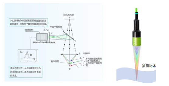
A chromatic confocal system uses a broadband light source and dispersive optics to focus different wavelengths at different positions along the measurement axis. The wavelength reflected from the target surface corresponds to a specific distance, allowing the system to calculate displacement with high accuracy.
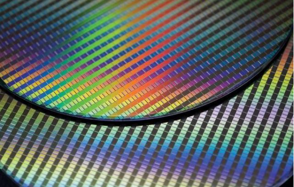
Because the method is optical and non-contact, it is well suited for delicate wafers, reflective films, transparent substrates, and microstructures where contact measurement may cause damage or instability.
Semiconductor Applications
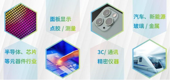
Typical applications include wafer thickness and TTV measurement, wafer warpage inspection, surface flatness detection, multilayer film thickness measurement, solder ball coplanarity, package height, pad height consistency, and microstructure height measurement.
LightE chromatic confocal technology helps semiconductor customers improve measurement reliability, reduce inspection risk, and build more stable process control for advanced manufacturing.