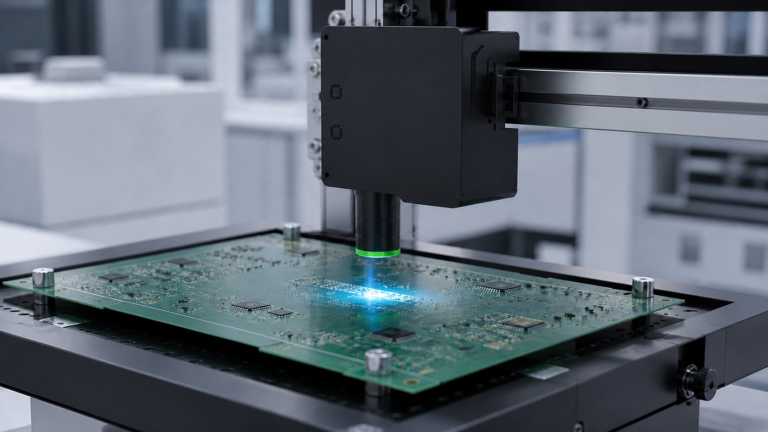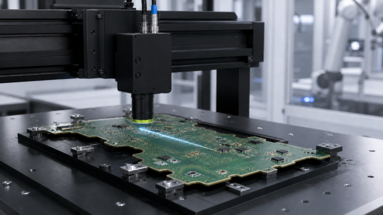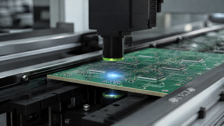
PCB thickness online detection PCB needs to strictly control the overall board thickness during the lamination and molding process. Contact measurement is inefficient and easy to damage the board surface.
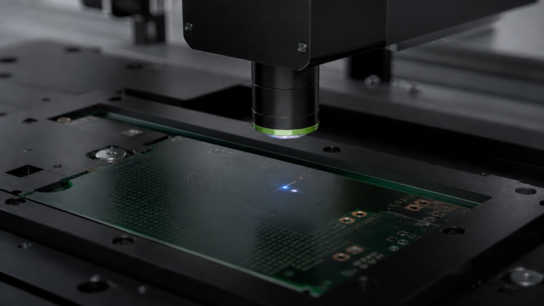
PCB flatness and warpage detection PCB is prone to warping after reflow soldering or heat treatment, which affects subsequent placement yield.
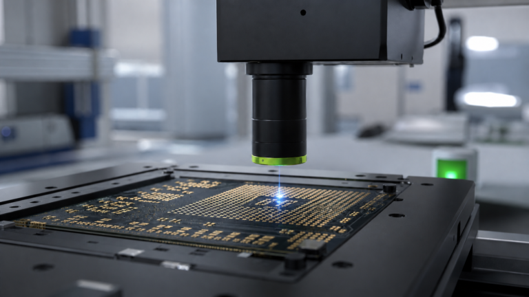
PCB pad height and coplanarity inspection Inconsistent pad heights can lead to weak soldering or poor soldering.
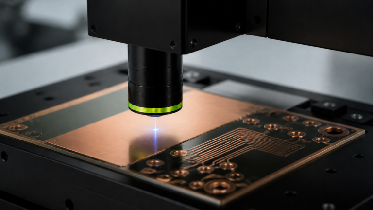
PCB copper foil and plating layer thickness detection The thickness of copper foil and electroplating layer directly affects the conductive performance and reliability, which requires high-precision and non-destructive testing.
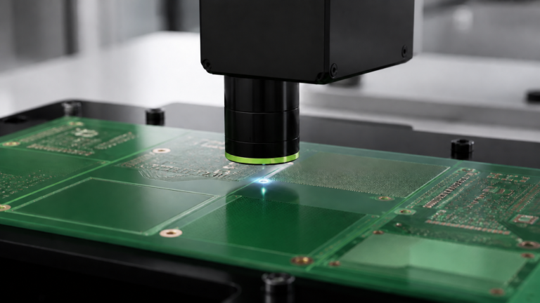
PCB solder mask and surface coating thickness inspection Uneven solder mask thickness can lead to soldering defects or insulation risks.
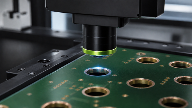
PCB drilling hole height and burr detection Burrs or abnormal height of the hole after drilling will affect the quality and reliability of plating.
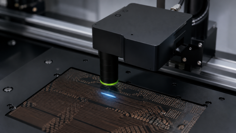
PCB line surface height and line width consistency detection Inconsistency between line height and line width will affect impedance and signal integrity.
Height detection of tiny defects on PCB surface Small defects such as scratches, dents, and residual copper are difficult to stably quantify through ordinary AOI.
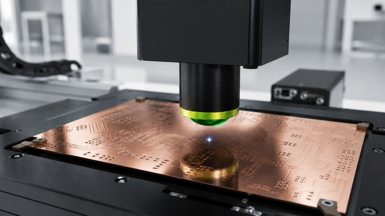
Non-contact measurement of highly reflective PCB surfaces High-gloss copper or plated surfaces reflect strongly to ordinary sensors, resulting in insufficient measurement stability.
Flexible PCB (FPC) thickness and deformation detection FPC is easy to bend and deform, and contact detection can easily cause damage.
Special-shaped PCB outline and height detection Special-shaped PCBs have complex shapes, and traditional inspection methods have low efficiency and poor consistency.