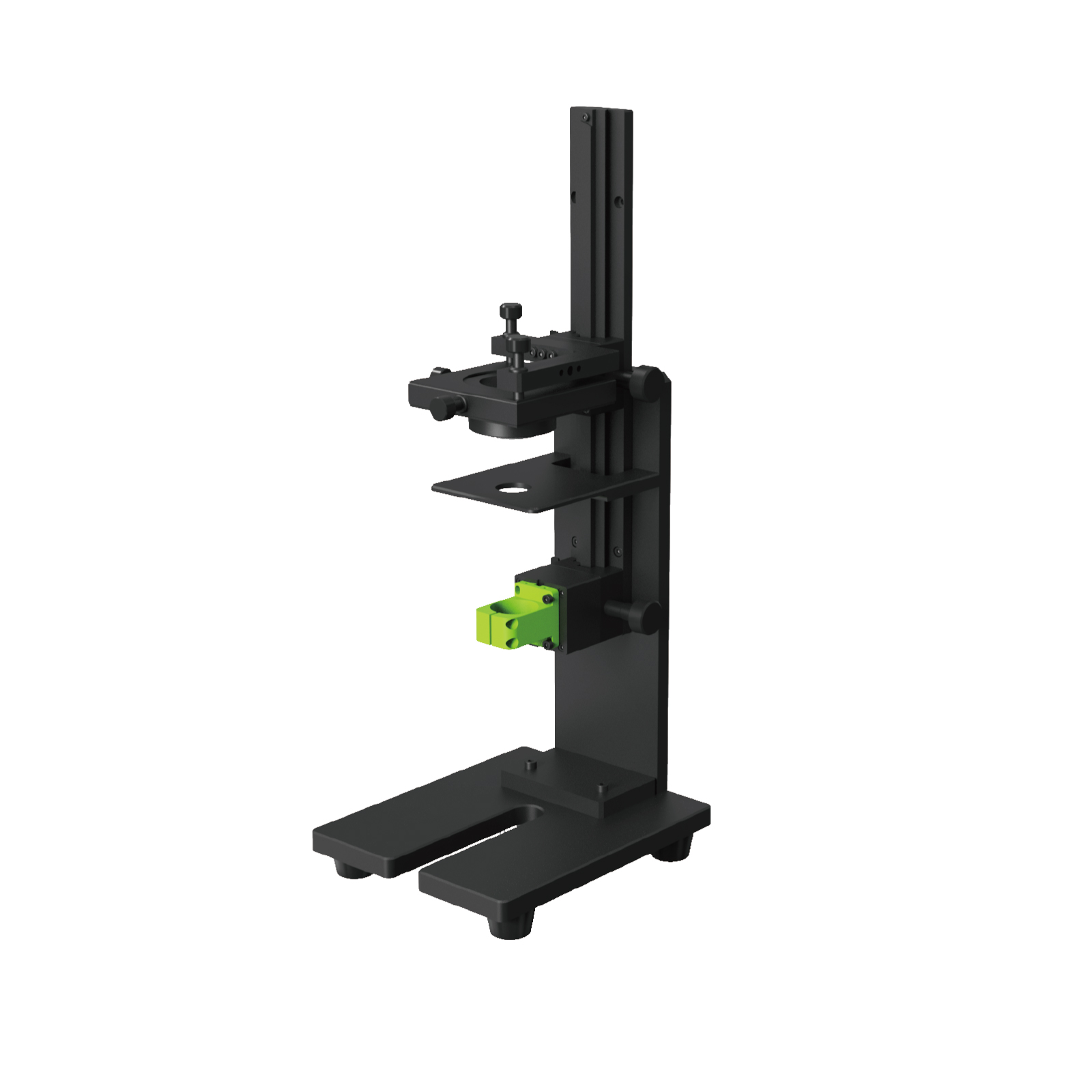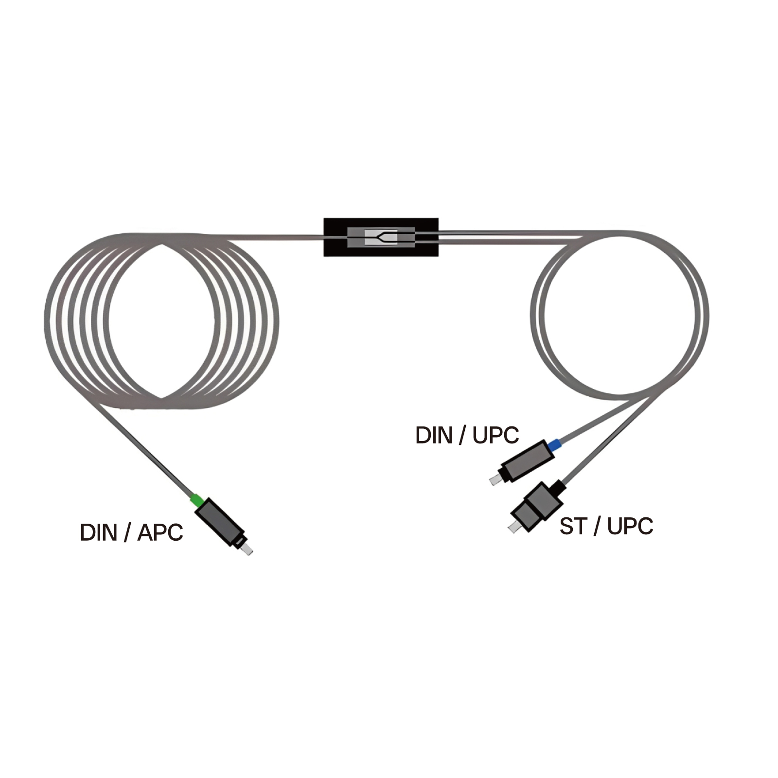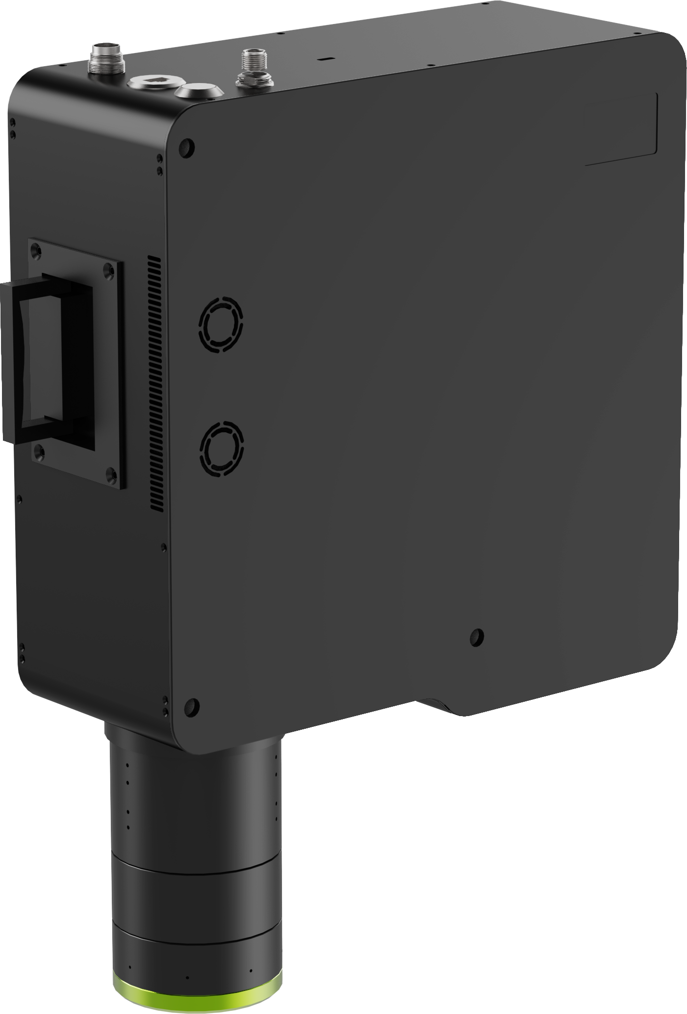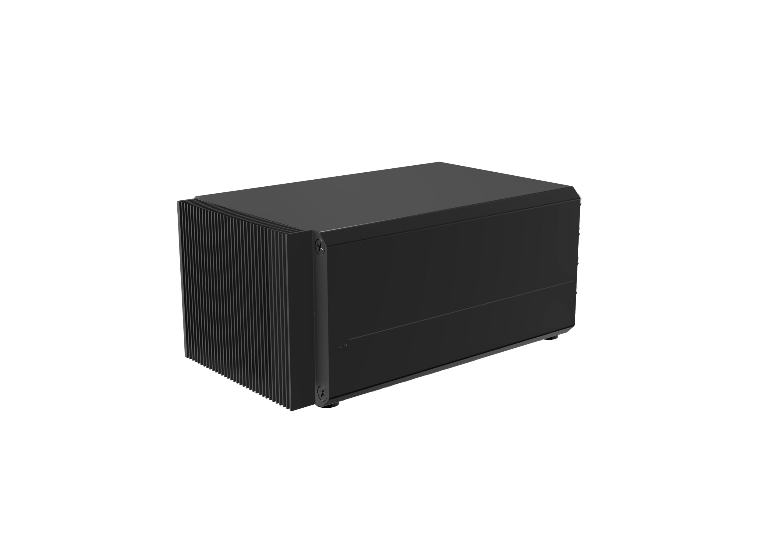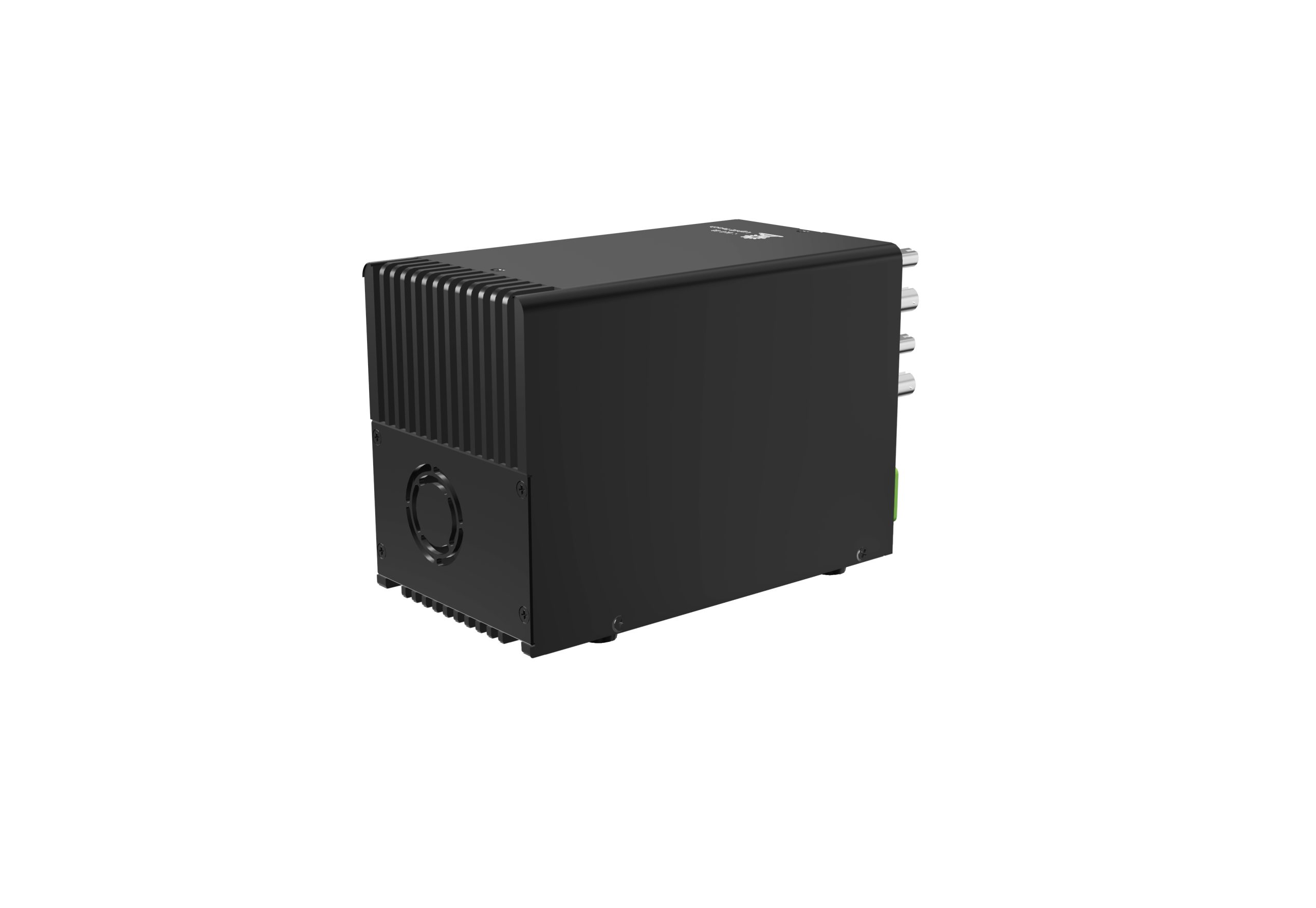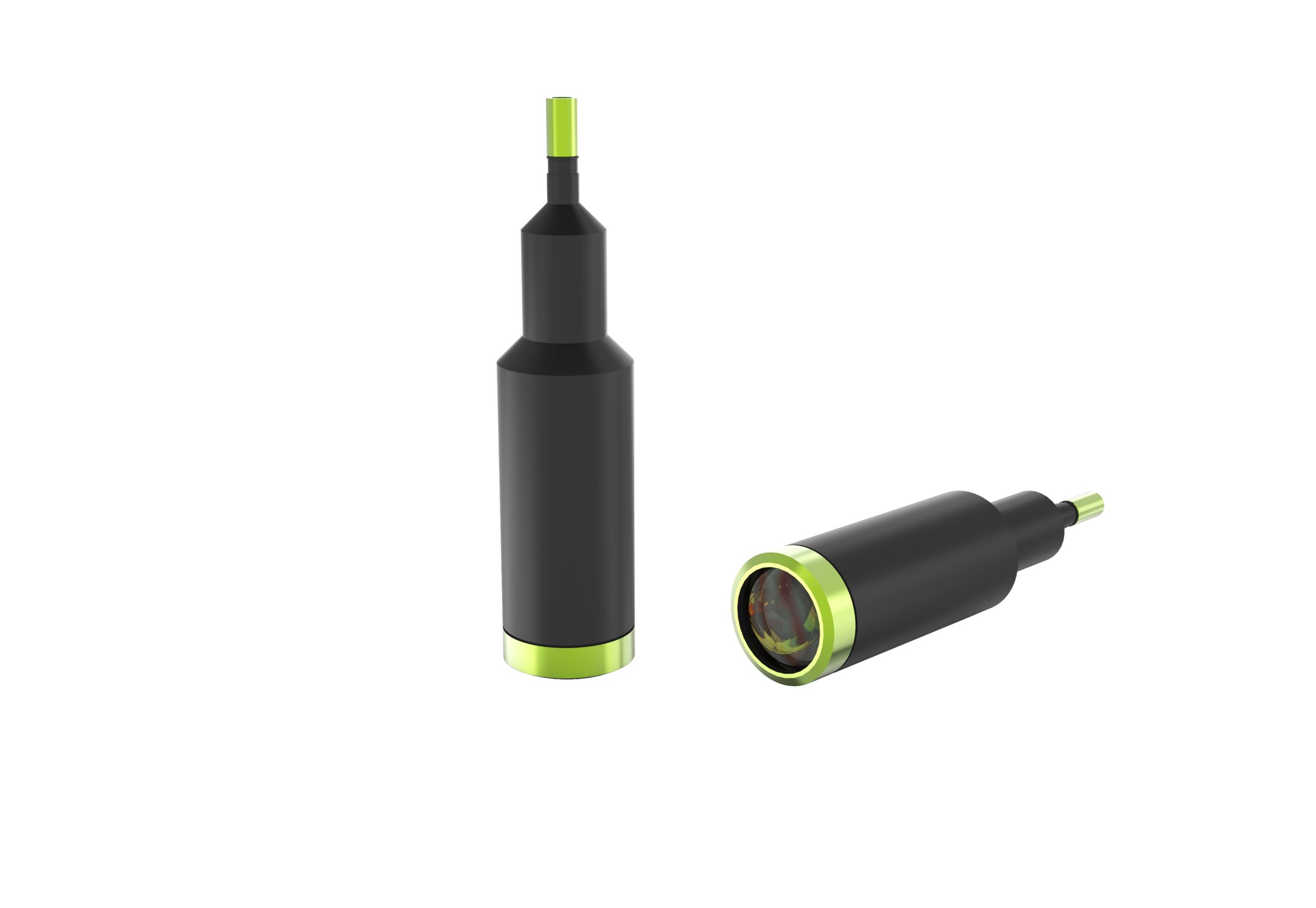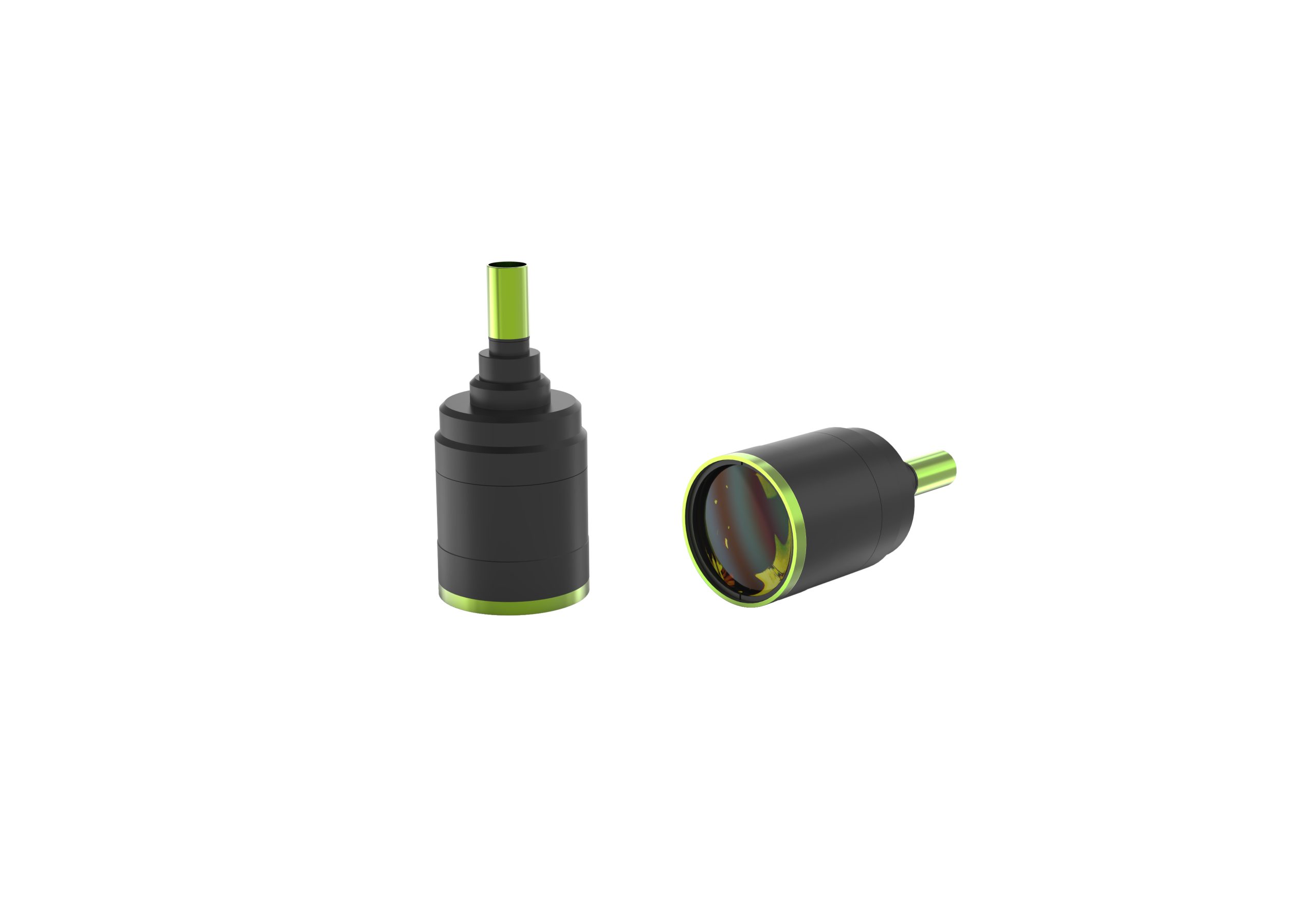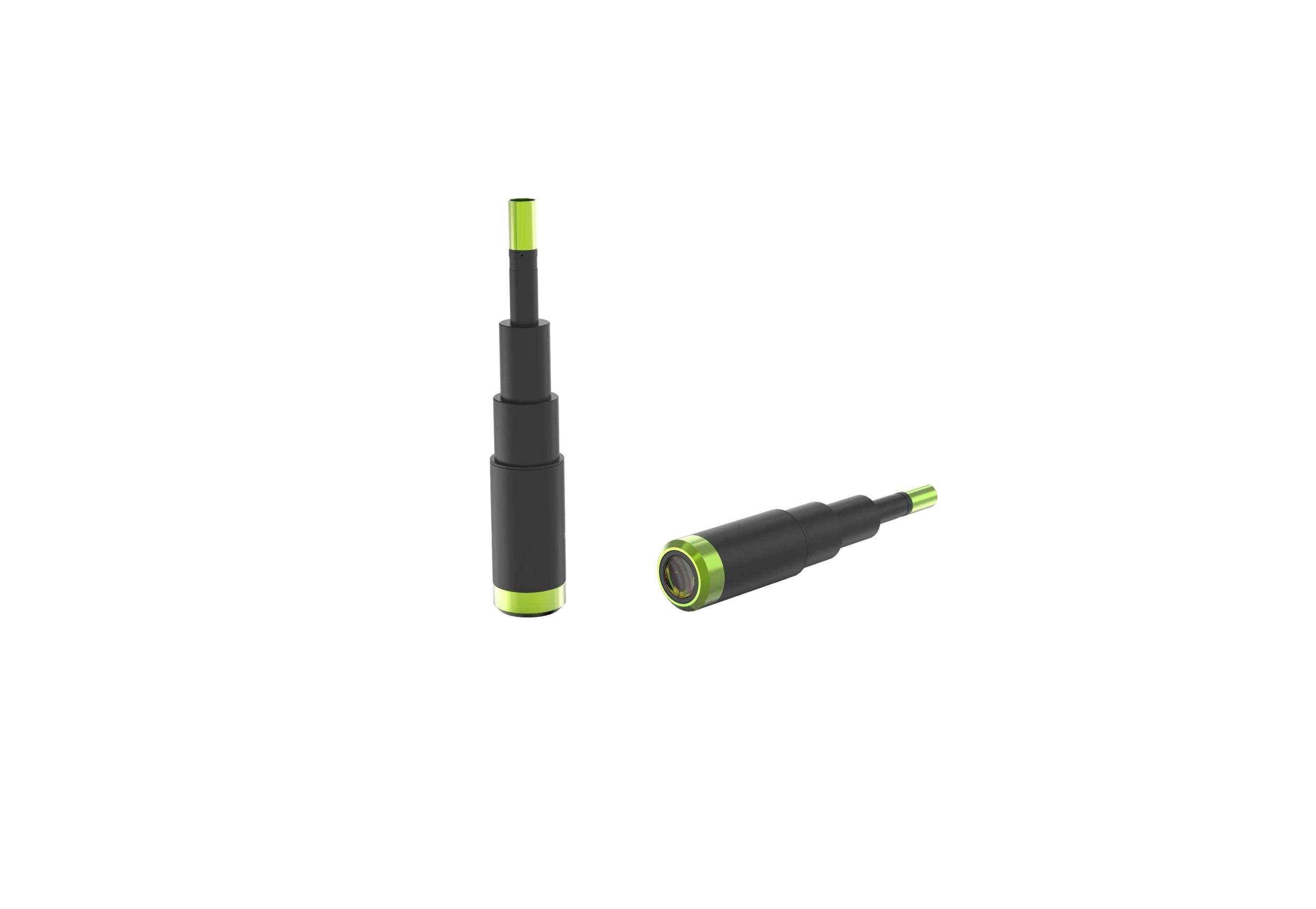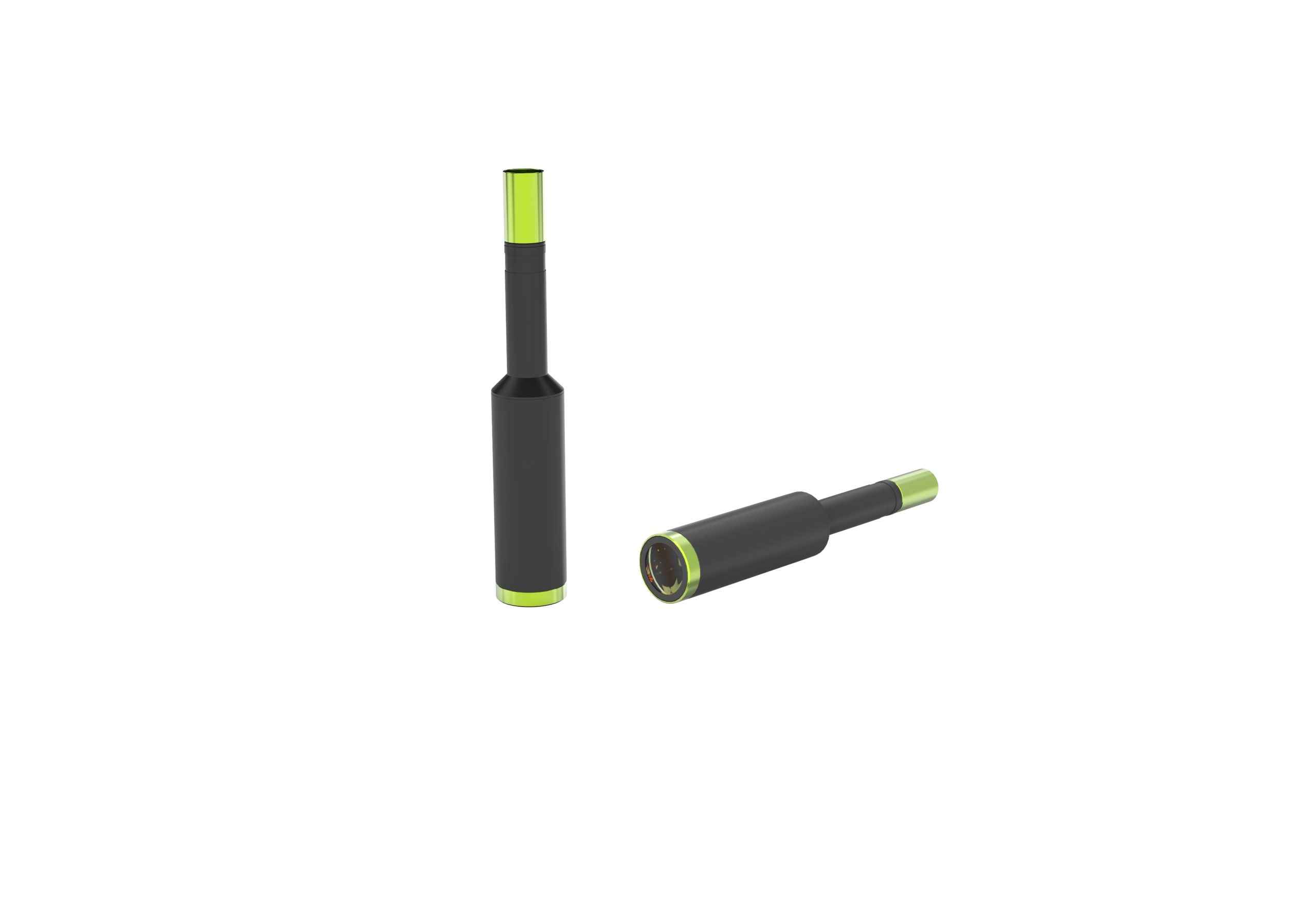
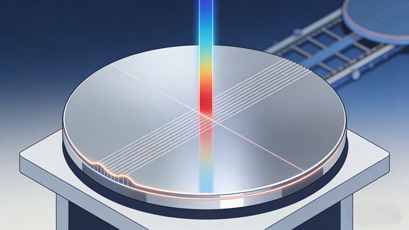
In the wafer manufacturing and thinning process, the overall thickness of the wafer and TTV (Total Thickness Variation) are key parameters that affect photolithography alignment and packaging yield. Traditional contact measurement is inefficient and carries the risk of scratching the wafer surface. LightE uses a non-contact optical measurement solution to perform high-precision height scanning on the wafer surface to achieve stable measurement of wafer thickness and TTV, ensuring measurement accuracy while avoiding damage to the wafer.
- 199 2531 7939
- mk7@lightegroup.com