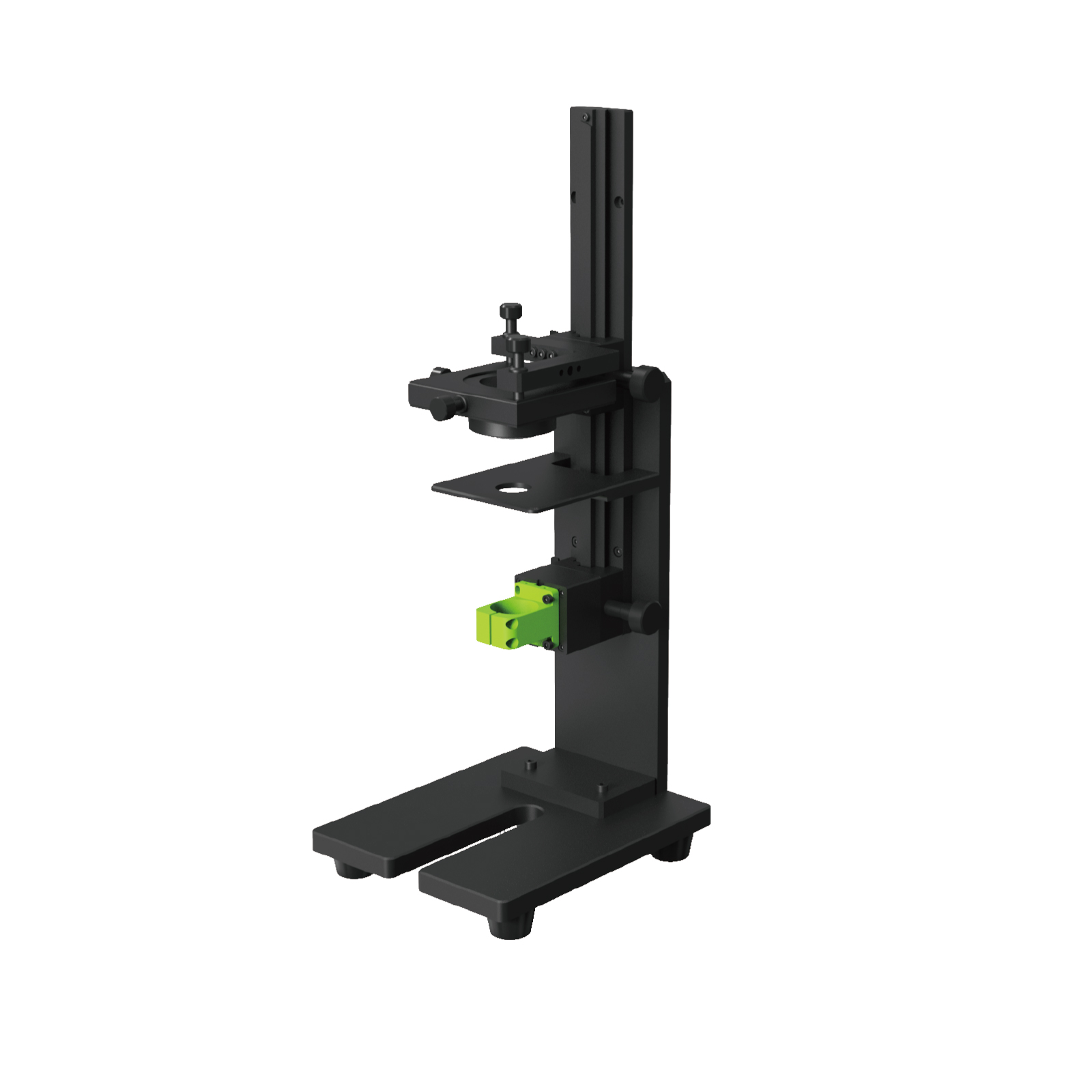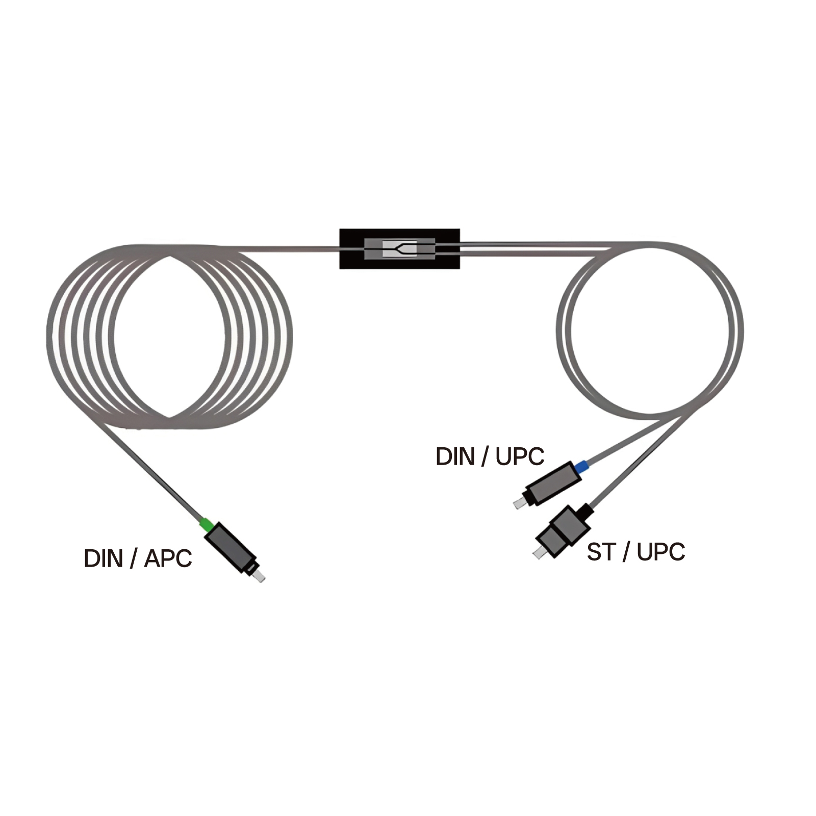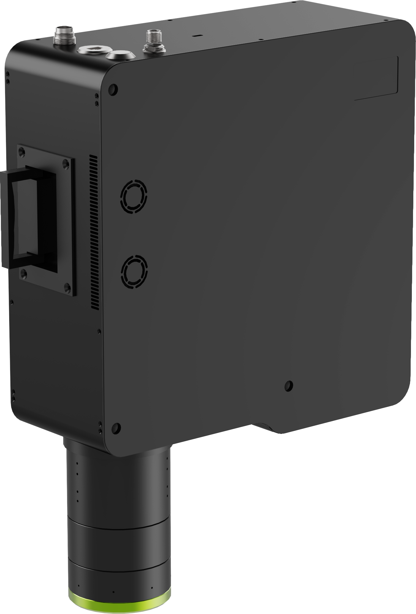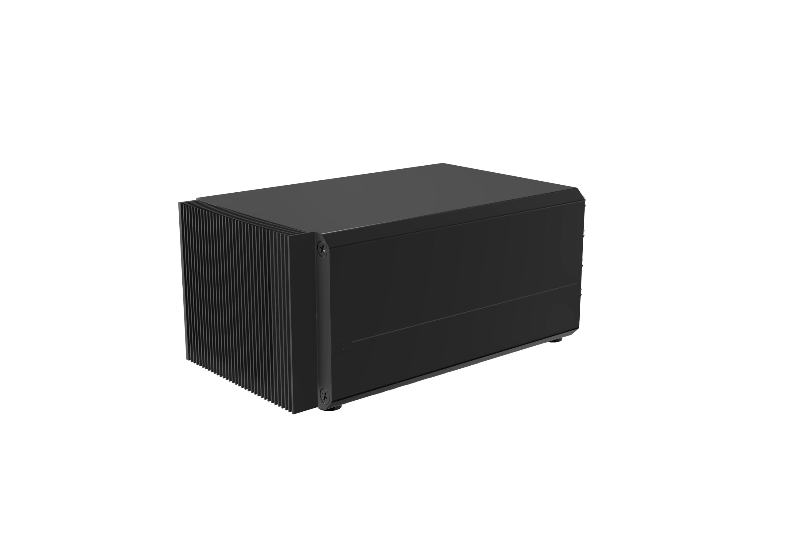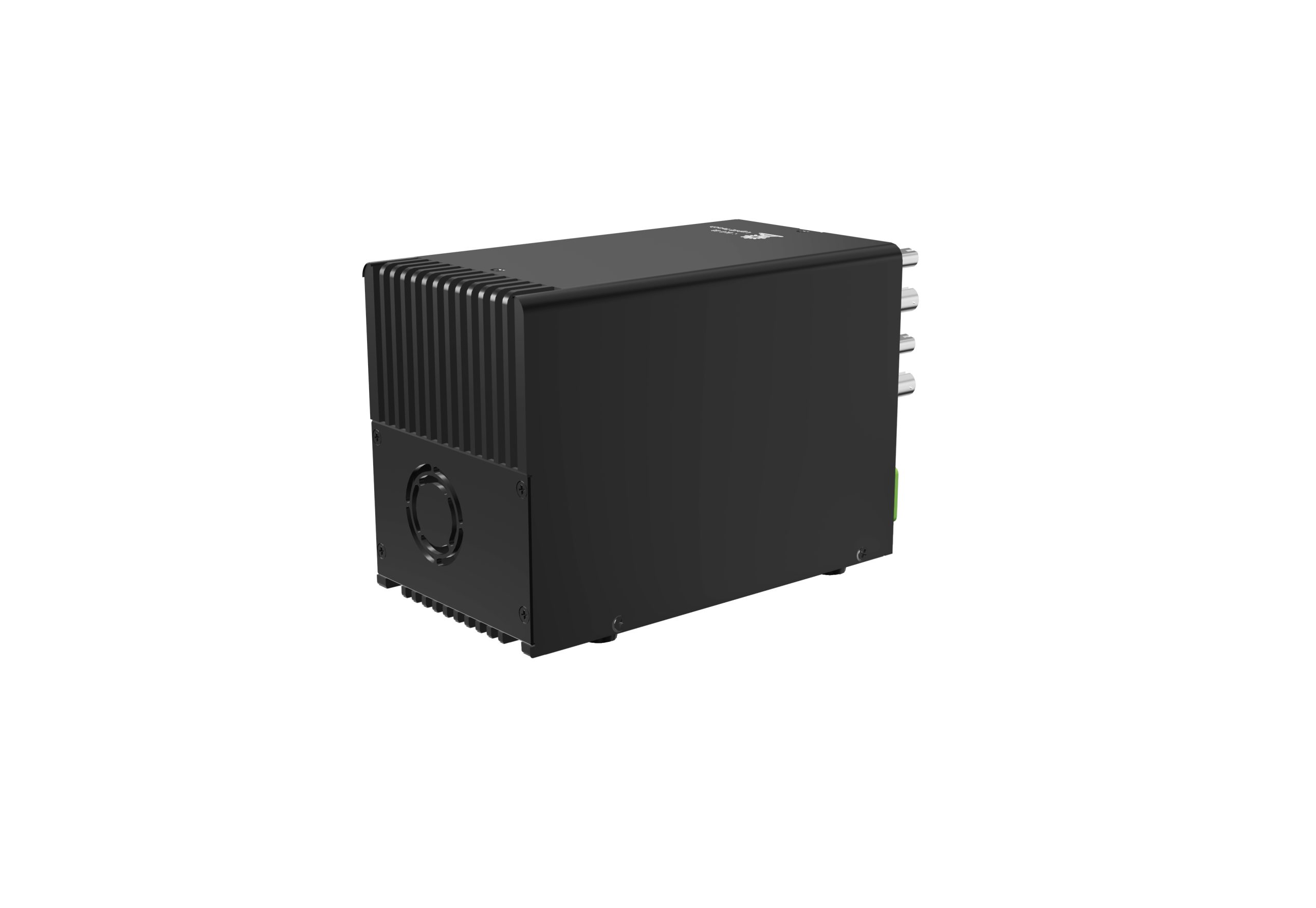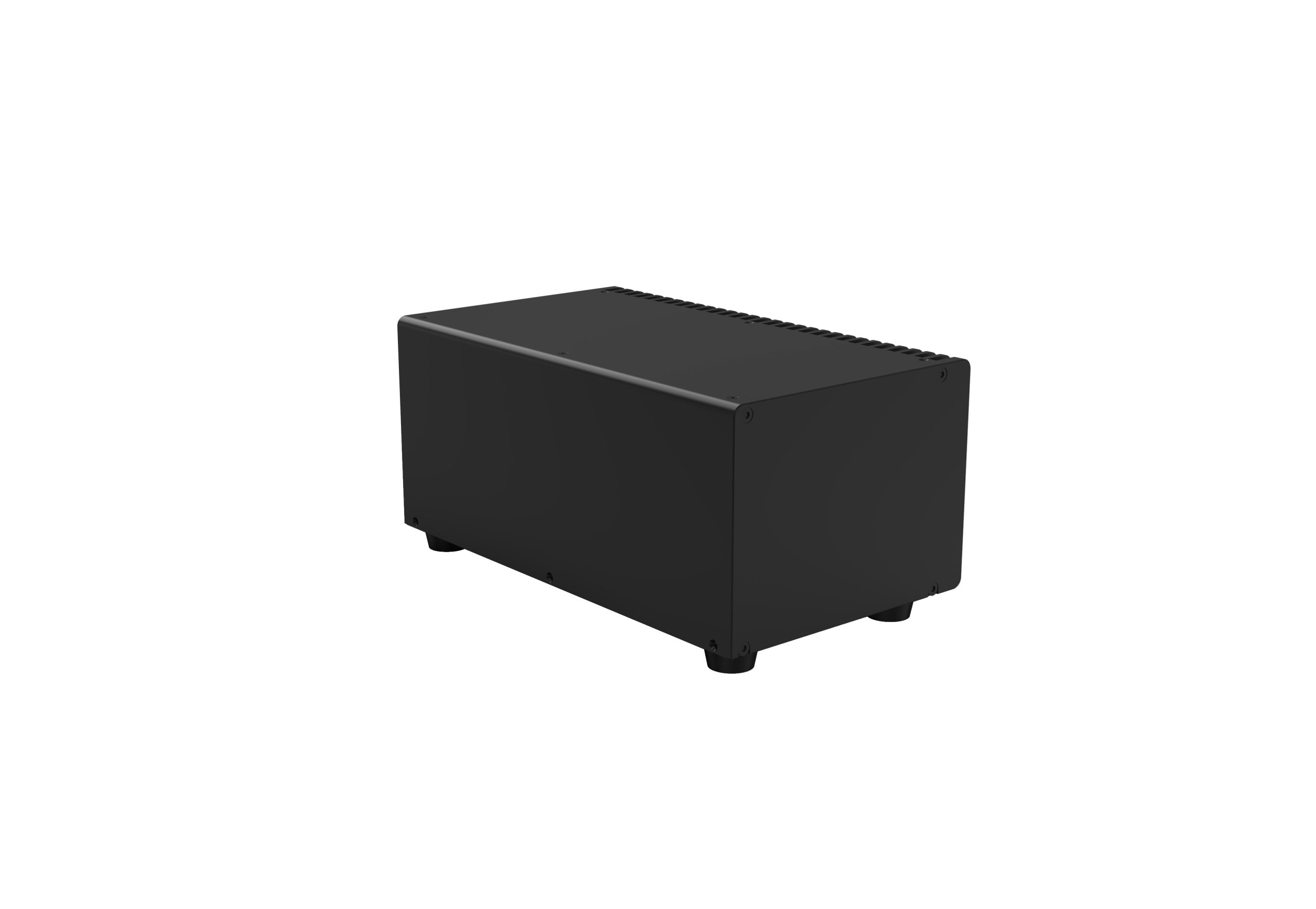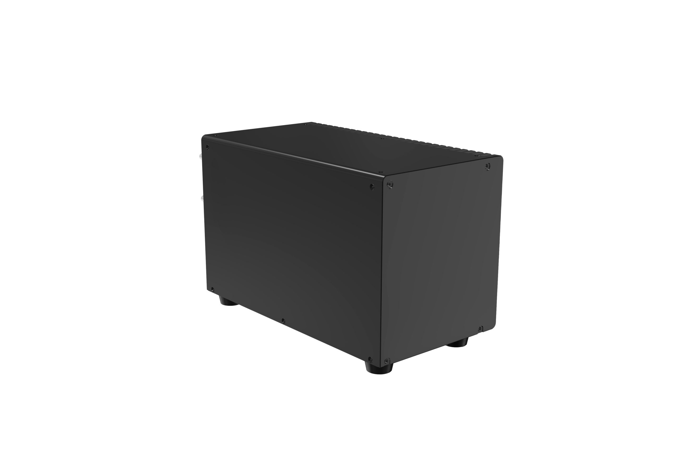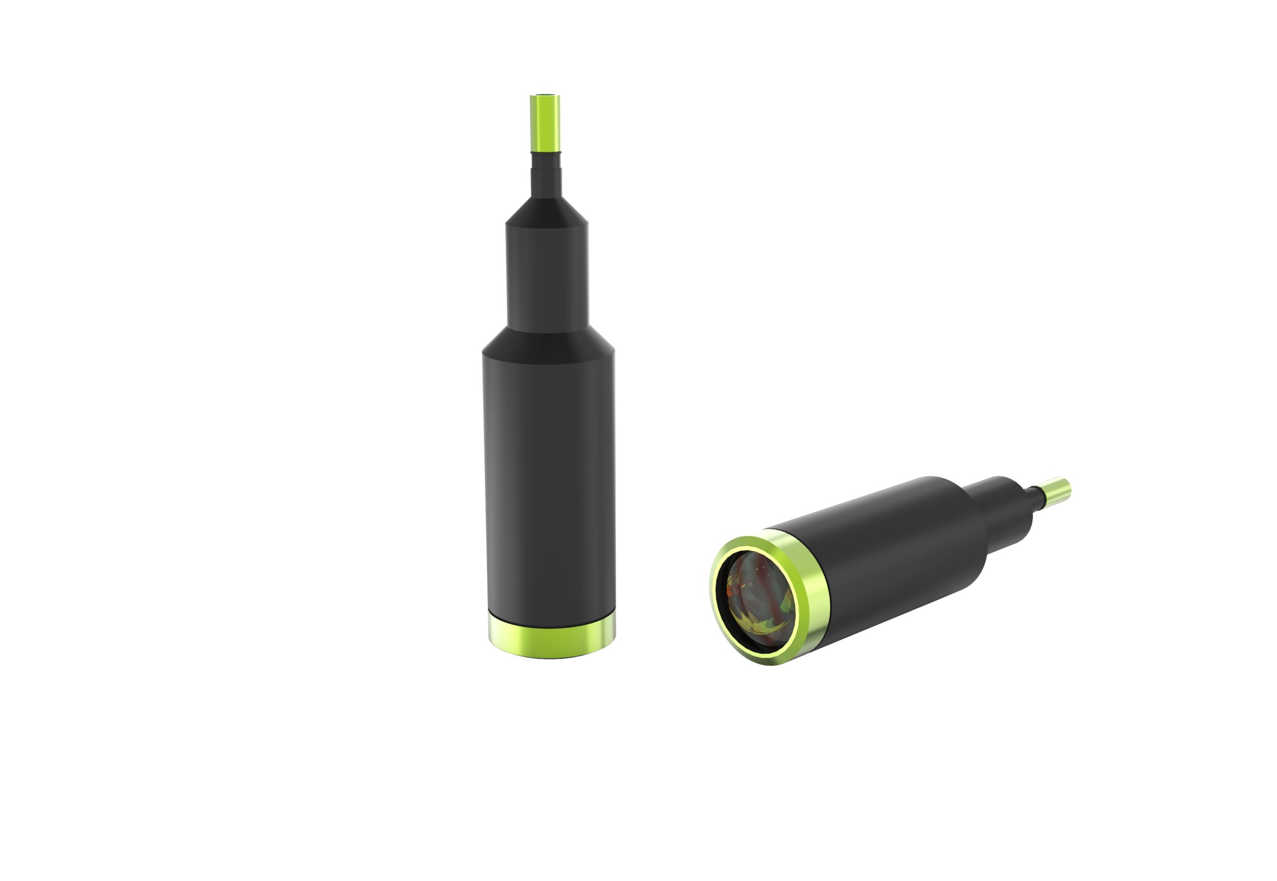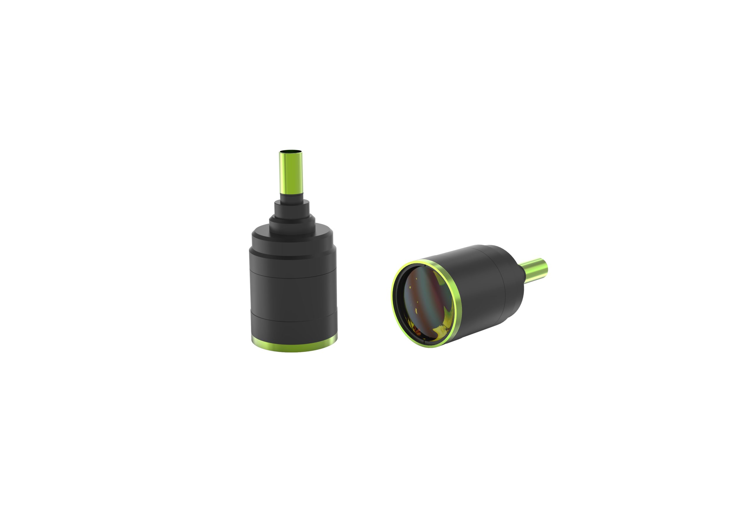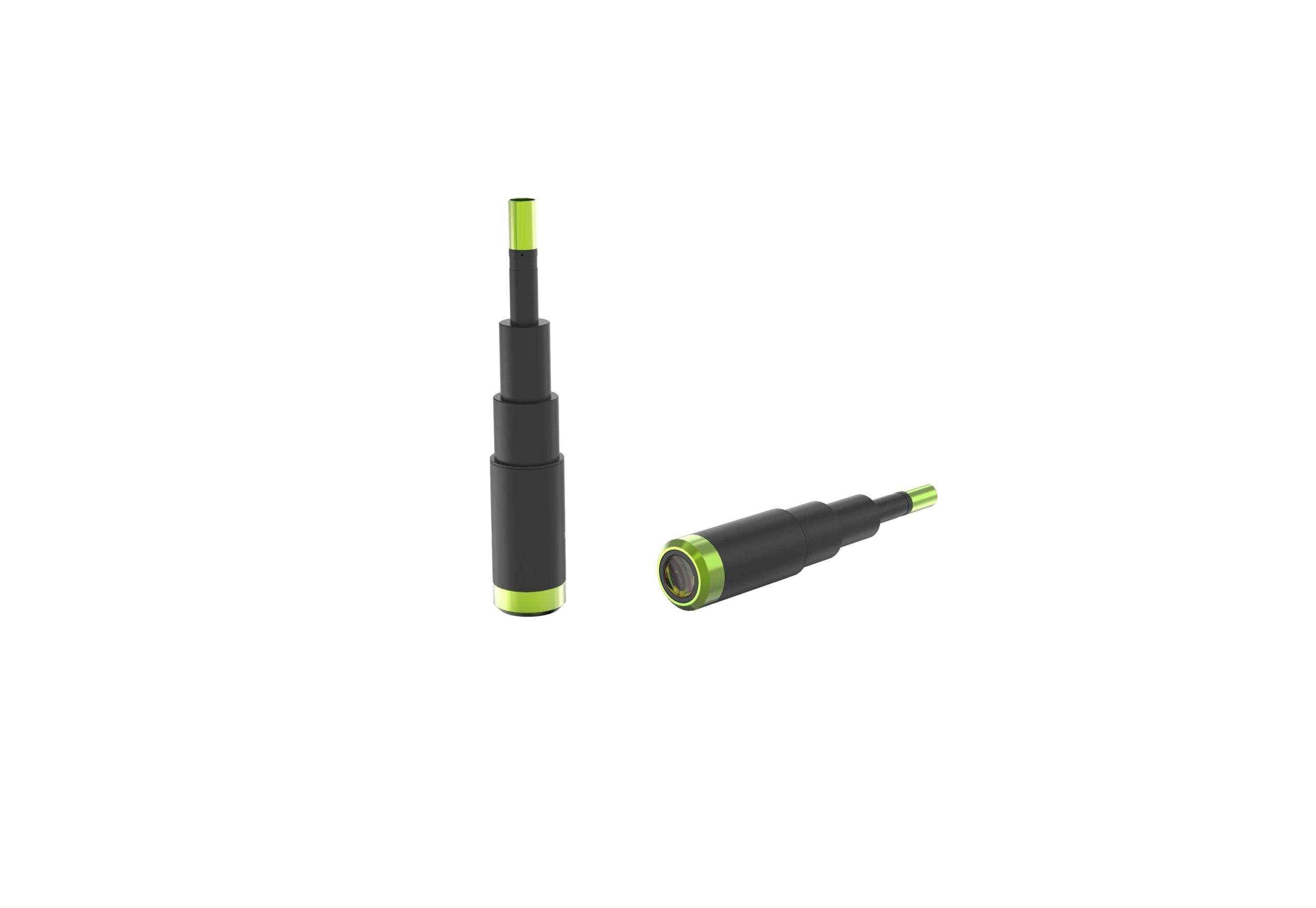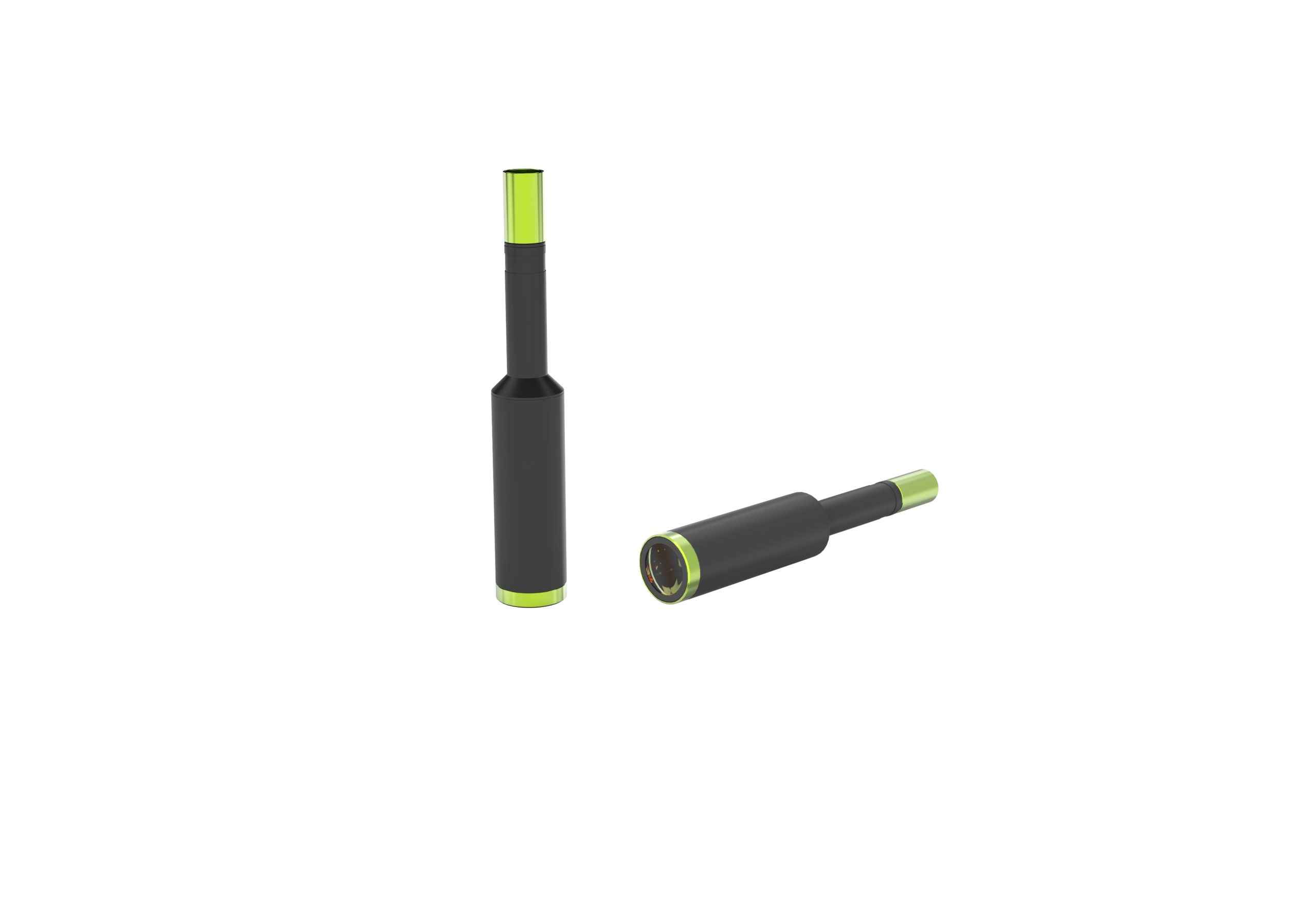
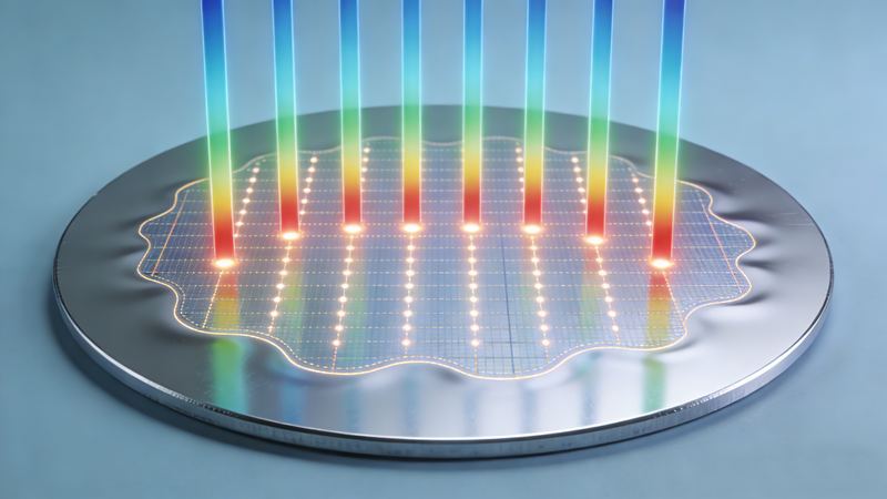
Wafer surface flatness directly affects photolithography focus accuracy and device consistency, and small topography changes may also cause process defects. LightE uses a non-contact high-resolution measurement solution to precisely scan the wafer surface to achieve stable detection of flatness and local topography, providing reliable data support for process optimization.
- 199 2531 7939
- mk7@lightegroup.com